Advanced materials
2D materials, perovskites and functional composites engineered for new electronic and photonic behaviour.
Discover
At Materials & Device Research Group, we connect advanced materials, optoelectronics and radiation detection to build technologies that sense, learn and respond.
 FIG. 01 / MATERIAL–DEVICE INTERFACE
01 — RESEARCH
Our work follows materials through the full translation pathway: synthesis, characterization, device fabrication, testing, and intelligent integration.
2D materials, perovskites and functional composites engineered for new electronic and photonic behaviour.
DiscoverPhotodetectors and imaging platforms spanning ultraviolet, visible, infrared and low-light operation.
DiscoverLead-free, high-sensitivity X-ray detectors designed for safer medical and industrial imaging.
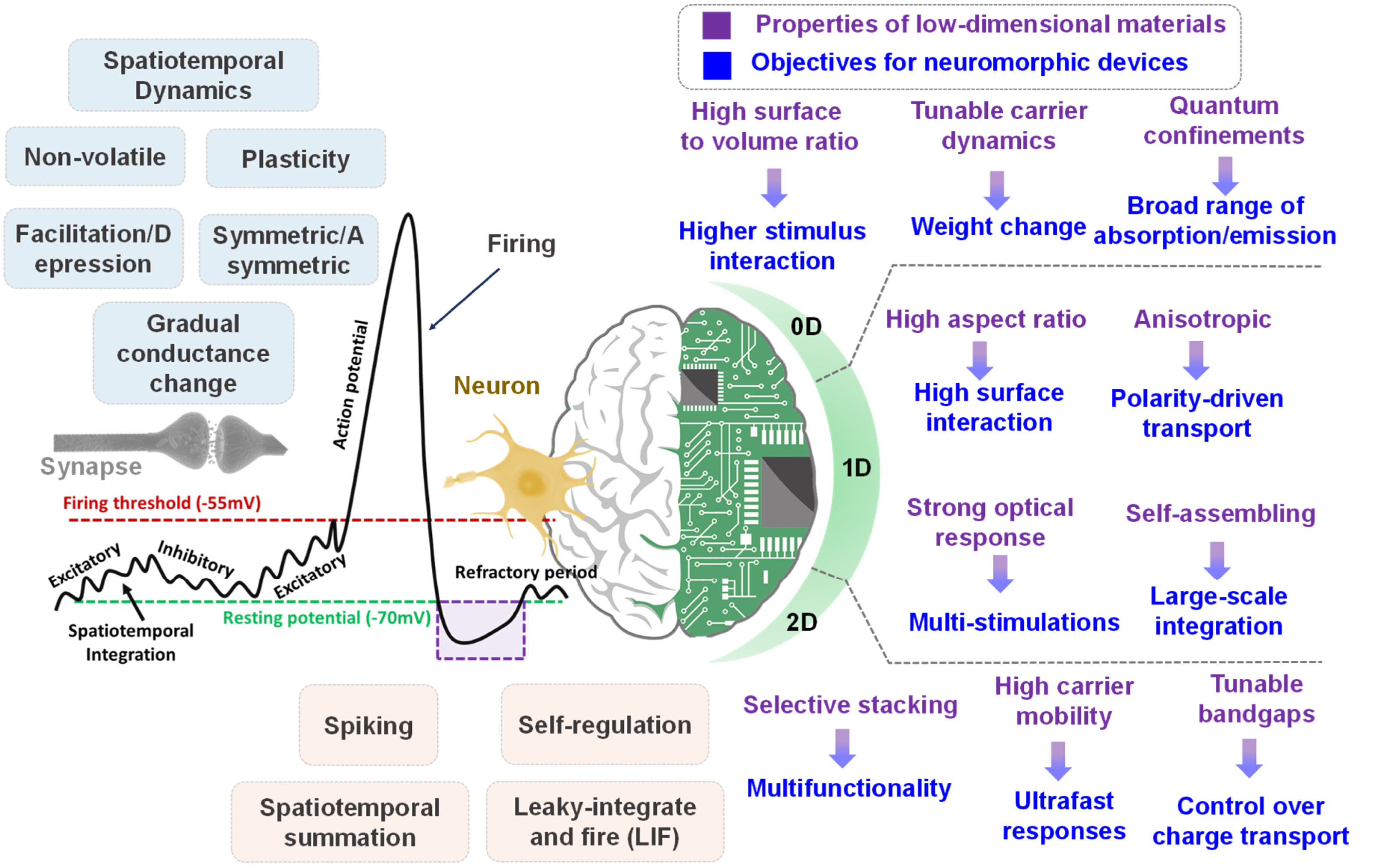
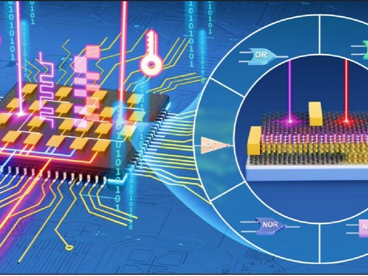
DiscoverNeuromorphic sensors and edge hardware that combine perception, memory and computation.
Discover02 — PEOPLE
Materials scientists, physicists, chemists and device engineers working as one team across disciplines and borders.
Work with usMaterials Science and Engineering: R: Reports
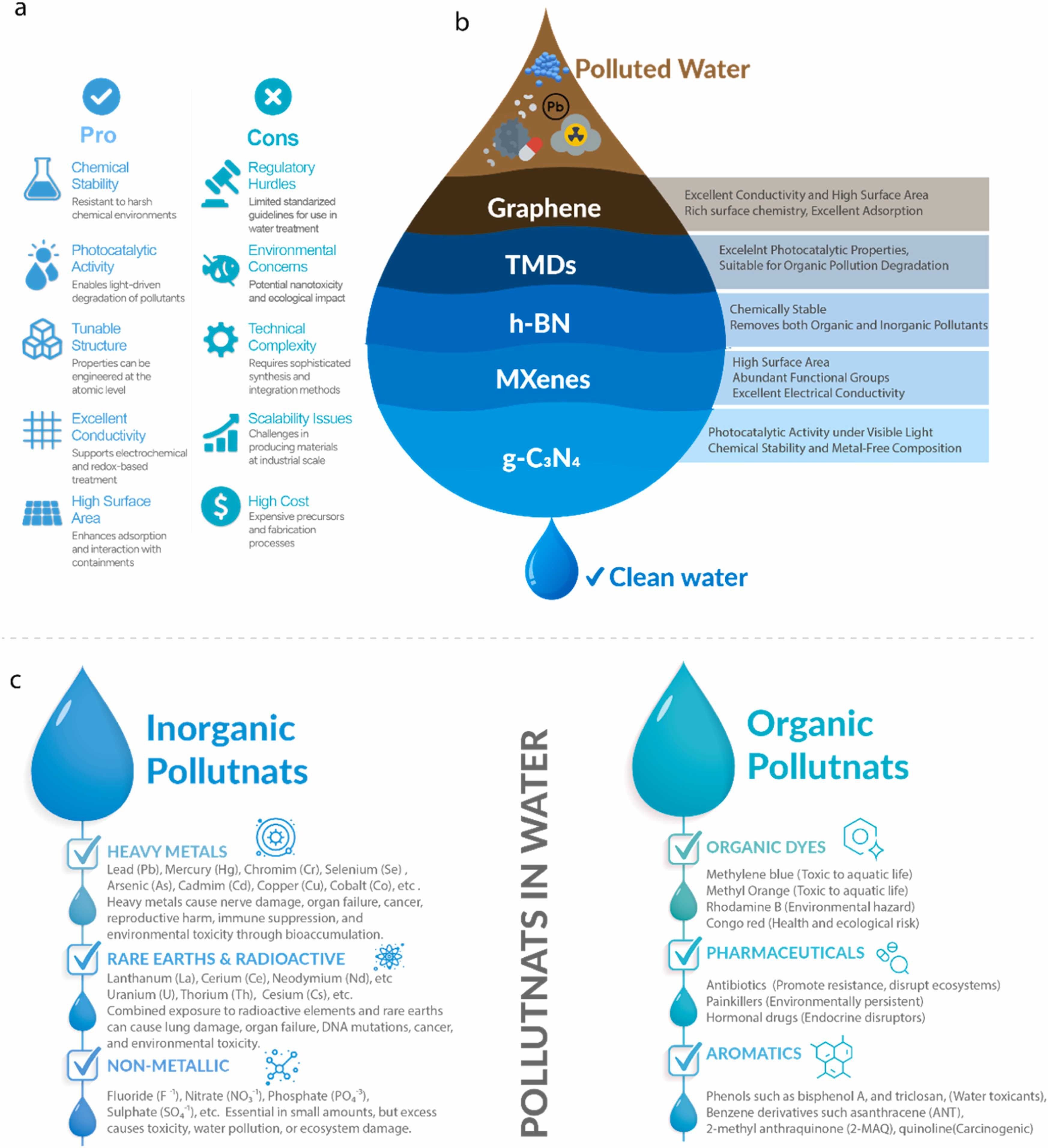
Chip
Small
04 — FACILITIES
Device fabrication
Optoelectronic testing
Surface characterization
Radiation detection
06 — OPPORTUNITIES
We welcome ambitious researchers who want to work across materials, devices and intelligent systems. Explore open positions or contact us with your own research idea.
View opportunitiesDevelop deep expertise while working on ambitious, internationally connected research.
Lead high-impact work in advanced optoelectronics and radiation-detector technologies.
Join us for focused exchanges, shared experiments and collaborative publications.
Build skills through projects, internships and interdisciplinary partnerships.